 ALLPCB
Xilinx FPGA BGA: NSMD vs SMD Pad Differences
Guide to Xilinx BGA pitches (1.0, 0.92, 0.8, 0.5mm): PCB layer estimation, NSMD vs SMD pads, via planning and routing tips.


Guide to Xilinx BGA pitches (1.0, 0.92, 0.8, 0.5mm): PCB layer estimation, NSMD vs SMD pads, via planning and routing tips.

EDA overview: tools, major global and Chinese vendors, and key chip design and manufacturing tool categories.
Learn PPA trade-offs and chip performance: bandwidth, throughput, latency explained with AXI, outstanding transactions, buffering and pipelining.
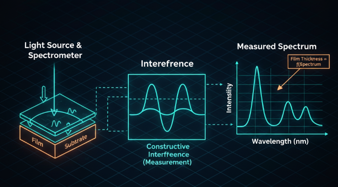
Learn thin film thickness measurement: four-point probe, ellipsometry & XRF to optimize semiconductor performance, yield and reliability.
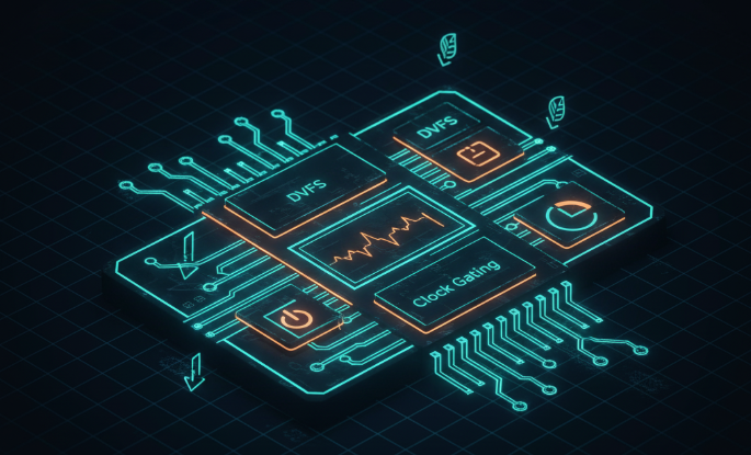
Explore low-power SoC design: techniques, dynamic vs static power, leakage, and subsystem impacts to extend battery life and reduce cost.
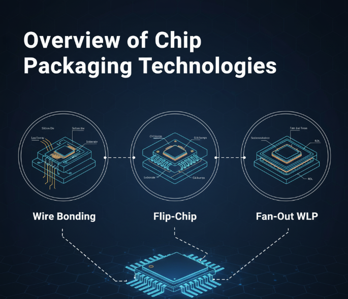
Semiconductor packaging guide: wire bonding, flip-chip, FOWLP, 2D/2.5D/3D multi-die, interposers, EMIB and FOCoS trade-offs
EDA overview: input methods, development stages, and goals to automate circuit design, simulation, verification, and system-level integration.
Explore chip design challenges from architecture to tape-out and verification, including frontend/backend, floorplanning and first-silicon testing.
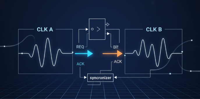
Single-bit sync across clock domains: handshake methods, pulse-loss issues, failure detection, plus Verilog examples for reliable transfers.
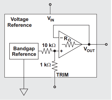
Reduce voltage reference noise with TRIM/noise pins (TI REF50xx), external caps, ESR tips or precision op-amp filters. Consult datasheet.

Explore chip power consumption sources and low-power design techniques, clock gating, DVFS, power gating, multi-voltage and layout optimizations.
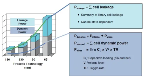
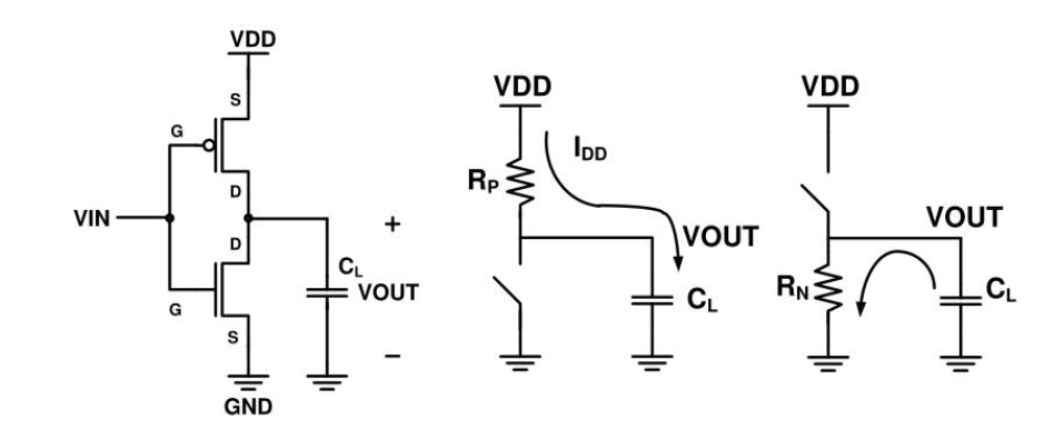
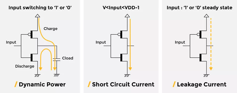
Explore chip power consumption, dynamic vs static power, and common digital IC techniques: clock/power gating, DVFS, multi-Vt and well biasing.
IC design explained: stages, CAD tools, verification, packaging, goals and applications from consumer electronics to automotive and medical devices.
Explore low-power IC design: dynamic vs static power, clock gating, voltage scaling, power switching, DVFS, multi-Vt and multi-voltage techniques.

Ansys power-integrity and multi-physics tools (Redhawk-SC, Totem, PathFinder-SC) support PI, SI and reliability signoff for Intel 16nm.
Low-power IC design techniques—voltage/clock management, power gating, sleep modes—and IC design flow from front-end to mass production.
EDA synthesis: converting HDL into optimized logic netlists. Learn types—logic, timing, physical, and power optimization—for IC design.
Learn how copper interconnects, low-k dielectrics, SOI, and HKMG enable reliable, high-performance 32/28nm CMOS scaling and advanced lithography.

Learn Coverage-Driven Verification (CDV) with UVM: testbench architecture, constrained-random testing, coverage collection, simulation and reuse.

Pipeline design: temporal parallelism, stage partitioning, throughput vs. latency trade-offs, and backpressure handling for efficient hardware.