ALLPCB


Overview
As process nodes advance (commonly 28nm, 22nm, 16nm, 14nm, and even 7nm), chip performance and scale have increased, making power consumption a critical concern for digital IC designers. Power requirements are especially strict for mobile consumer electronics, where excessive power dissipation can degrade product performance or cause thermal issues. This article reviews the definition and components of chip power consumption and summarizes common techniques to reduce power.
Power Composition
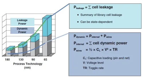
Chip power consumption is generally divided into two parts: dynamic power and static power.
Dynamic power
Dynamic power is the energy consumed when a circuit is switching. For CMOS circuits it can be further divided into switching power and short-circuit power. Switching power charges the load capacitance when a gate switches, while short-circuit power occurs during input transitions when PMOS and NMOS conduct simultaneously for a brief interval. This can be expressed as:
Pdyn = (CL * Vdd2 * Ptran * F) + (ttran * Vdd * Ipeak * F)
Where CL is the total load capacitance of the circuit; Vdd is the supply voltage; Ptran is the fraction of the circuit switching; F is the clock frequency; ttran is the overlap conduction time of PMOS and NMOS; and Ipeak is the peak short-circuit current. The first term represents switching power and the second term represents short-circuit power. In practice, if gate slew is sufficiently fast (ttran small), short-circuit power is often negligible.
From the expression above, strategies to reduce dynamic power include lowering Vdd, reducing F, reducing CL, and reducing the number of gate transitions.
Static power
Static power is the leakage current when transistors are not switching. Key contributors include:
- Subthreshold leakage Isub: current flowing from drain to source through the weak inversion channel.
- Gate leakage Igate: current from gate to substrate through the thin gate oxide due to tunneling and hot carrier effects.
- Gate-induced drain leakage IGIDL: current from drain to substrate induced by the strong electric field at the drain.
- Reverse-bias junction leakage Irev: current from drain or source to substrate due to minority carrier diffusion and generation in the depleted junction.
Common Techniques to Reduce Power in Digital IC Design
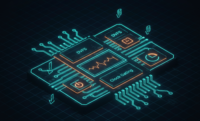
- Clock gating. Clock signals toggle frequently and can account for roughly 20–30% of chip power. Clock gating disables the clock to modules that are not in use by using a control signal, reducing their switching activity. Clock gating can be inserted at RTL (root-level gate cells) or automatically added by synthesis tools. From a front-end perspective, placing clock gating closer to the root can control more registers or clock domains and save more power. However, root-level gating can create timing closure challenges for the gating enable pin (for example, the gating enable pin Epin), which may be difficult to meet during implementation.
- Power gating. In back-end design, power gating reduces leakage by inserting switches such as MTCMOS to disconnect power to standard cell blocks when they are idle.
- Multi-Vt cells. Use high-Vt (HVT) or regular-Vt (RVT) cells in non-critical paths to reduce leakage. This requires trade-offs with timing, performance, and area, since HVT/RVT cells can make timing closure more difficult and may impact area optimization.
- DVFS. Dynamic Voltage and Frequency Scaling adjusts supply voltage and clock frequency according to workload requirements. This ensures sufficient performance while avoiding excessive power delivery. For example, a CPU cluster can be overdriven to higher voltage for peak performance or underdriven to lower voltage for power savings when lower frequency suffices.
- Well biasing. Dynamically adjusting well bias voltages can reduce leakage and thus lower static power.