ALLPCB


Hard gold plating is a critical process in PCB manufacturing, especially for applications requiring high durability and reliable electrical connectivity. However, engineers often encounter challenges like uneven coatings, adhesion issues, and wear over time. If you're searching for solutions to hard gold plating problems, this guide offers a detailed troubleshooting roadmap. From identifying common defects to providing actionable repair strategies, we’ve got you covered with practical insights tailored for engineers. Let’s dive into the specifics of hard gold plating defects, failure analysis, and effective troubleshooting techniques to ensure your projects meet the highest standards.
What is Hard Gold Plating and Why Does It Matter?
Hard gold plating is an electroplating process that deposits a durable layer of gold onto a substrate, typically used in printed circuit boards (PCBs) for connectors, edge contacts, and other high-wear areas. Unlike soft gold, hard gold is alloyed with small amounts of other metals like cobalt or nickel to enhance its hardness and wear resistance. This makes it ideal for applications where components face repeated mechanical stress, such as in edge connectors that endure thousands of mating cycles—often up to 20,000 cycles without significant wear.
The importance of hard gold plating lies in its ability to provide excellent corrosion resistance, low contact resistance (typically below 50 milliohms), and consistent signal integrity. However, when issues arise, they can lead to costly failures in electronic devices. Understanding and addressing hard gold plating problems is crucial for maintaining performance and reliability in critical applications like aerospace, medical devices, and telecommunications.
Common Hard Gold Plating Problems and Defects
Despite its advantages, hard gold plating is not immune to issues. Below, we outline the most frequent hard gold plating defects engineers encounter, along with their potential causes. Recognizing these problems early can save time and resources during production.
1. Uneven Thickness or Poor Coverage
Uneven thickness in hard gold plating often appears as patchy or inconsistent layers across the surface. This defect can compromise electrical conductivity and wear resistance, especially in high-contact areas. Measurements using a thickness gauge might reveal variations outside the acceptable range of 0.75 to 1.25 micrometers for typical hard gold applications.
Causes: Poor bath agitation, incorrect current density (often below the recommended 1-5 A/dm2), or contamination in the plating solution can lead to uneven deposition.
2. Poor Adhesion or Peeling
Adhesion issues occur when the gold layer separates from the substrate, often visible as peeling or flaking. This defect can result in exposed base metal, increasing the risk of corrosion and signal loss.
Causes: Inadequate surface preparation, such as insufficient cleaning or improper activation of the substrate, is a common culprit. Residual oxides or organic contaminants on the surface can prevent proper bonding.
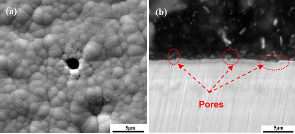
3. Porosity and Pinholes
Porosity manifests as tiny holes or voids in the gold layer, which can allow moisture or corrosive agents to reach the underlying material. This defect often leads to failure in harsh environments, reducing the lifespan of the component.
Causes: High current density (above 10 A/dm2) during plating or impurities in the gold solution can create porous layers. Hydrogen gas entrapment during the process may also contribute to pinholes.
4. Discoloration or Tarnishing
Hard gold plating should maintain a bright, uniform appearance. Discoloration, such as a reddish or brownish hue, indicates potential issues with the plating process or contamination, often linked to alloy imbalances or oxidation.
Causes: Incorrect pH levels in the plating bath (optimal range is typically 3.5-4.5) or exposure to contaminants like sulfur compounds can cause tarnishing.
5. Excessive Wear or Abrasion
While hard gold is designed for durability, premature wear can occur in high-friction applications, leading to thinning of the gold layer and exposure of the base material. This can increase contact resistance beyond acceptable limits, such as above 100 milliohms after wear testing.
Causes: Insufficient hardness due to improper alloy composition or plating thickness below the minimum specification (e.g., less than 0.5 micrometers) can accelerate wear.
Hard Gold Plating Troubleshooting Guide: Step-by-Step Solutions
Addressing hard gold plating issues requires a systematic approach. This troubleshooting guide provides actionable steps to identify root causes and implement fixes for the defects mentioned above. Use these strategies to optimize your plating process and minimize failures.
Step 1: Evaluate Plating Bath Conditions
Start by checking the chemical composition of the plating bath. Ensure gold concentration is within the recommended range (typically 2-4 g/L for hard gold solutions). Test for contaminants using analytical methods like atomic absorption spectroscopy if available. Maintain pH levels between 3.5 and 4.5, and keep bath temperature stable (around 50-60°C) to avoid deposition inconsistencies.
Step 2: Optimize Current Density and Agitation
Adjust the current density to match the manufacturer’s specifications, usually between 1 and 5 A/dm2 for hard gold plating. Too high a current can cause burning or porosity, while too low a current results in uneven coverage. Ensure proper agitation using mechanical stirrers or air bubbling to maintain uniform ion distribution in the bath.
Step 3: Improve Surface Preparation
Before plating, thoroughly clean the substrate to remove oils, oxides, and residues. Use a multi-step cleaning process, including degreasing with alkaline solutions, acid pickling to remove oxides, and a final rinse with deionized water. For better adhesion, consider an activation step using a strike layer, such as a thin nickel coating, before applying the gold layer.
Step 4: Monitor Plating Thickness
Use non-destructive testing methods like X-ray fluorescence (XRF) to measure gold layer thickness across multiple points on the component. Target a uniform thickness of 0.75-1.25 micrometers for most hard gold applications. If variations are detected, adjust plating time or current distribution to achieve consistency.
Step 5: Conduct Regular Bath Maintenance
Filter the plating solution regularly to remove particulates and organic impurities. Replace or replenish the bath as needed based on usage and test results. Monitor the alloying elements (like cobalt or nickel) to ensure the hardness of the gold layer meets specifications, typically around 150-200 Knoop hardness.
Hard Gold Plating Repair: Fixing Defects Post-Production
Sometimes, defects are only discovered after the plating process is complete. While prevention is ideal, hard gold plating repair is possible in many cases. Here’s how to address common issues without scrapping the entire component.
Repairing Uneven Thickness
For areas with insufficient gold thickness, selective re-plating can be applied. Mask off unaffected areas using non-conductive tape or resist, then re-plate the deficient sections using a brush plating technique. Ensure the bath conditions match the original process to avoid mismatch in appearance or performance.
Fixing Adhesion Issues
If peeling is localized, carefully strip the affected gold layer using a mild chemical stripper compatible with the substrate. Clean and re-prepare the surface as described earlier, then re-plate the area. For widespread adhesion failure, it may be more cost-effective to strip and redo the entire plating.
Addressing Porosity
Porous layers often cannot be repaired directly. If the porosity is minor, applying a thin overcoat of gold may seal small voids. However, for significant porosity, stripping and re-plating is recommended to ensure reliability, especially for components exposed to harsh environments.
Hard Gold Plating Failure Analysis: Identifying Root Causes
Failure analysis is a critical step in preventing recurring hard gold plating problems. By systematically investigating defects, engineers can refine processes and improve outcomes. Here’s how to conduct a thorough failure analysis.
1. Visual and Microscopic Inspection
Begin with a detailed visual inspection under magnification (10x to 50x) to identify defects like cracks, pinholes, or discoloration. Document findings with high-resolution images for reference during analysis.
2. Thickness and Composition Testing
Use XRF or cross-sectional microscopy to measure gold thickness and check for alloy composition deviations. Compare results against specifications to determine if under- or over-plating contributed to the failure.
3. Adhesion and Hardness Testing
Perform adhesion tests using methods like tape testing or bend testing to evaluate bonding strength. Measure hardness using a microhardness tester to confirm if the gold layer meets the required durability (150-200 Knoop).
4. Environmental and Stress Testing
Simulate operating conditions by subjecting the plated component to thermal cycling (e.g., -40°C to 85°C for 100 cycles) or corrosion testing (e.g., salt spray for 48 hours). Monitor for degradation to identify if environmental factors played a role in the failure.
5. Process Audit
Review plating process logs to check for deviations in parameters like current density, bath temperature, or cleaning procedures. Cross-reference with defect patterns to pinpoint procedural errors.
Preventive Measures for Long-Term Success
Preventing hard gold plating issues starts with proactive measures during design and manufacturing. Incorporate these best practices to minimize defects and ensure consistent quality.
- Design for Plating: Avoid sharp edges or complex geometries that can cause uneven current distribution during plating. Use rounded corners on edge connectors to promote uniform gold deposition.
- Specify Clear Requirements: Define precise thickness and hardness specifications in your design documentation. For example, specify a gold thickness of 0.75-1.25 micrometers and hardness of 150-200 Knoop for high-wear applications.
- Partner with Experts: Collaborate with experienced plating providers who use advanced quality control measures, such as real-time bath monitoring and automated thickness testing.
- Routine Testing: Implement in-process inspections, including thickness measurements and adhesion tests, to catch issues early in the production cycle.
Conclusion: Mastering Hard Gold Plating Challenges
Hard gold plating is a powerful solution for enhancing the durability and performance of PCB components, but it comes with its share of challenges. By understanding common hard gold plating problems like uneven thickness, poor adhesion, and porosity, engineers can take proactive steps to troubleshoot and repair defects effectively. This practical guide has walked you through identifying hard gold plating defects, applying targeted fixes, conducting failure analysis, and implementing preventive measures to ensure long-term success.
With the right approach to hard gold plating troubleshooting, you can achieve reliable, high-quality results that meet the demands of even the most critical applications. Keep this guide handy as a reference for tackling hard gold plating issues and refining your processes for optimal performance.