ALLPCB


Overview
Some voltage reference ICs include a dedicated noise-reduction pin. These pins allow filtering of reference noise to achieve improved performance. Different references may require different external circuits for effective noise filtering; there is no one-size-fits-all solution. Before applying any filtering technique, carefully review the device datasheet for specific guidance.
TI REF50xx Series with a TRIM/Noise Pin
The REF50xx family from TI provides a TRIM pin connected to the bandgap output, which permits connecting an external capacitor to form a low-pass filter at the bandgap output. The simplified block diagram is shown below.
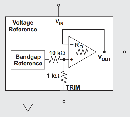
There are two main noise sources: the bandgap reference and the output buffer/op amp. Connecting a 1 μF capacitor to the TRIM pin is reported to reduce total output RMS noise by about 2.5×. An additional capacitor can be placed at the VOUT pin to form a second low-pass stage. Adding both capacitors yields the schematic shown below, suitable for 8- to 14-bit data converters.
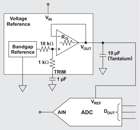
The equivalent series resistance (ESR) of the output capacitor (for example a 10 μF capacitor) is important because it is connected to the output of the internal op amp that uses a feedback path. If the ESR is very low (around 0.1 Ω), the feedback network is effectively tied to a large capacitive load. Driving a large load capacitance can reduce op amp phase margin and produce gain peaking. According to TI documentation, an ESR of roughly 1.5 Ω can avoid stability issues. For more background on why a relatively larger ESR can stabilize a feedback amplifier driving a large capacitive load.
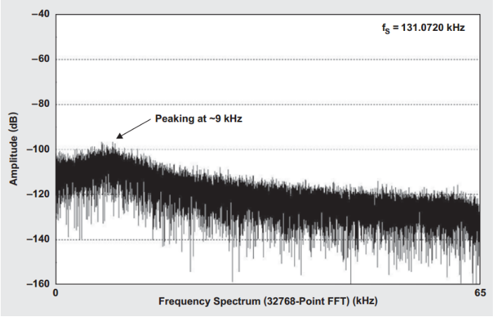
Note that increased gain peaking will cause larger noise at the reference output, as illustrated below.
Given these interactions, always consult the voltage reference datasheet before implementing any external filtering.
Voltage References without a Noise-Reduction Pin
For references that lack a dedicated noise pin, use a precision op amp to implement an external low-pass filter. A typical topology places a single-pole low-pass formed by R2 and C2 at the output of a precision amplifier, as shown below. This prevents the voltage reference IC from having to drive a large capacitive load directly.
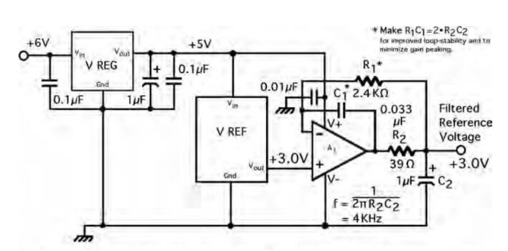
Although the filter attenuates noise from both the reference and the amplifier, the chosen op amp must have very low noise, low offset, and low drift. Use low-TC precision resistors and high-quality polypropylene capacitors for best long-term stability. A low-noise linear regulator can provide clean supply rails for the reference and the amplifier. Selecting R1*C1 = 2*R2*C2 can improve loop stability for this filter topology.
Other Techniques
The two techniques described above are not the only options for suppressing voltage reference noise. More complex filter topologies can be used in place of the single-pole filter.