ALLPCB


In the fast-paced world of electronics, designing high-frequency PCBs (Printed Circuit Boards) requires precision and a deep understanding of signal behavior. But how can you create layouts that not only perform well at high frequencies but also embrace sustainability? This blog dives into the key considerations for high-frequency PCB design, focusing on impedance control, signal integrity, dielectric materials, and stack-up design, all while integrating sustainable practices to reduce environmental impact.
Whether you're an engineer working on cutting-edge 5G applications or designing high-speed digital circuits, this guide will walk you through actionable strategies to optimize your PCB layouts. Let’s explore how to balance performance with eco-friendly design choices for a greener future in electronics.
Why Sustainable High-Frequency PCB Design Matters
High-frequency PCB design is critical for applications like telecommunications, automotive radar, and IoT devices, where signals operate at frequencies above 1 GHz. At these speeds, even small layout errors can lead to signal loss, interference, or complete failure. Meanwhile, sustainability in electronics is no longer just a trend—it’s a necessity. The industry is under pressure to minimize waste, reduce energy consumption, and use eco-friendly materials without compromising performance.
By combining sustainable practices with high-frequency design principles, you can create PCBs that meet modern performance demands while contributing to a healthier planet. Let’s break down the core elements of this approach.
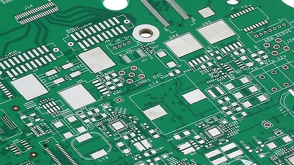
Key Considerations for High-Frequency PCB Design
Designing for high frequencies involves tackling challenges like signal degradation, electromagnetic interference (EMI), and impedance mismatches. Below are the critical factors to consider, paired with sustainable strategies to enhance your layout process.
1. Impedance Control: The Backbone of Signal Performance
Impedance control is essential in high-frequency PCB design to ensure signals travel without distortion. Mismatched impedance can cause reflections, leading to data errors or signal loss. For example, a common target impedance for high-speed digital signals is 50 ohms, often used in USB or Ethernet applications.
To achieve proper impedance control:
- Maintain consistent trace widths and spacing: Use precise calculations to match the impedance of traces to the target value. For a 50-ohm trace on a standard FR-4 material with a dielectric constant (Dk) of 4.2, a trace width of about 6 mils might be required for a 1.6mm thick board.
- Minimize vias: Vias introduce inductance and can disrupt impedance. When unavoidable, use back-drilling to remove unused via stubs that cause signal reflections.
- Choose sustainable materials: Opt for lead-free laminates and eco-friendly surface finishes like immersion silver, which reduce hazardous waste compared to traditional options.
2. Signal Integrity: Ensuring Clean Data Transmission
Signal integrity refers to the quality of an electrical signal as it travels through the PCB. At high frequencies, issues like crosstalk, noise, and timing errors become more pronounced. Poor signal integrity can result in bit errors or system failures, especially in applications like 5G or high-speed computing.
Here are practical tips to maintain signal integrity:
- Avoid sharp bends in traces: Sharp corners can cause signal reflections. Instead, use 45-degree angles or curved traces to maintain smooth signal flow.
- Implement ground planes: A solid ground plane beneath signal traces reduces EMI and provides a stable return path. Ensure the ground plane is continuous, without splits or gaps.
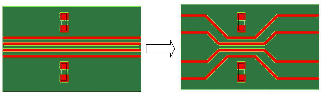
- Space traces to prevent crosstalk: Follow the 3W rule, where the spacing between parallel traces is at least three times the trace width, to minimize electromagnetic coupling.
- Sustainable routing: Optimize trace lengths to reduce material usage. Shorter traces not only improve signal integrity by minimizing delay but also cut down on copper consumption.
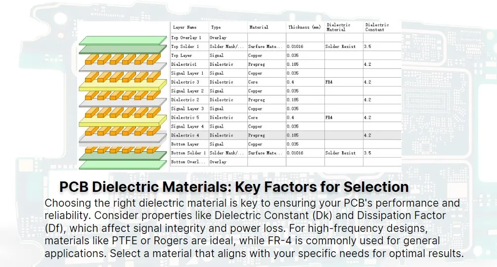
3. Dielectric Materials: Choosing the Right Foundation
The choice of dielectric material significantly impacts high-frequency performance. Dielectric constant (Dk) and dissipation factor (Df) determine how signals propagate through the board. Materials with a lower Dk allow faster signal speeds, while a low Df reduces signal loss.
For high-frequency designs, consider these material properties:
- FR-4 alternatives: Standard FR-4 has a Dk of around 4.2, which may not be ideal for frequencies above 1 GHz due to higher losses. Instead, use materials like Rogers RO4350B with a Dk of 3.48 and lower loss tangent for better performance at 5 GHz and beyond.
- Temperature stability: High-frequency applications often experience thermal stress. Choose materials with stable Dk across temperature ranges to maintain consistent impedance.
- Eco-friendly options: Look for halogen-free laminates that avoid toxic flame retardants. These materials reduce environmental harm during manufacturing and disposal.
Selecting the right dielectric material is a balancing act between performance, cost, and sustainability. Always evaluate the specific frequency requirements of your project before deciding.
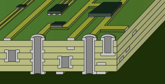
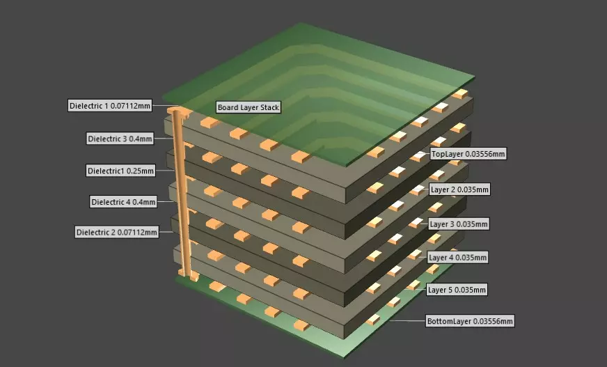
4. Stack-Up Design: Building a Solid Structure
PCB stack-up design defines the arrangement of signal, ground, and power layers in a multilayer board. A well-planned stack-up is crucial for managing signal integrity, EMI, and thermal performance in high-frequency designs.
Key principles for effective stack-up design include:
- Symmetrical layering: Arrange layers symmetrically to prevent warping during manufacturing. For a 6-layer board, a common stack-up might be Signal-Ground-Signal-Power-Ground-Signal.
- Ground plane proximity: Place ground planes close to signal layers to minimize loop inductance and provide effective shielding. A spacing of 5 mils between a signal layer and ground plane can significantly reduce noise.
- Power integrity: Dedicate layers for power distribution and use decoupling capacitors near ICs to stabilize voltage levels, especially in high-speed circuits operating at 3.3V or lower.
- Sustainable stack-ups: Minimize the number of layers where possible to reduce material usage and manufacturing energy. Optimize designs to use fewer layers without sacrificing performance.
A carefully designed stack-up not only boosts signal performance but also contributes to a more sustainable manufacturing process by reducing waste.
Sustainability in High-Frequency PCB Layout
Sustainability is a growing priority in electronics design. By integrating eco-friendly practices into high-frequency PCB layouts, you can reduce environmental impact while maintaining top-tier performance. Here are some actionable ways to make your designs greener.
1. Material Selection for a Greener Future
Choosing sustainable materials is a powerful step toward reducing the environmental footprint of PCB production. Focus on:
- Lead-free solders: Avoid lead-based solders to comply with regulations like RoHS (Restriction of Hazardous Substances) and minimize toxic waste.
- Recyclable substrates: Use substrates that can be recycled at the end of the product lifecycle, reducing landfill waste.
- Low-energy manufacturing materials: Select laminates and finishes that require less energy to process, cutting down on carbon emissions.
2. Efficient Design to Minimize Waste
Efficient PCB layouts can significantly cut down on material waste during production. Consider these strategies:
- Optimize panelization: Arrange multiple PCB designs on a single panel to maximize material usage and reduce scrap during fabrication.
- Reduce over-engineering: Avoid unnecessarily large boards or excessive layers. Design with the exact specifications needed for your high-frequency application to save resources.
- Digital simulation: Use simulation tools to test signal integrity and impedance control before prototyping. This reduces the need for multiple physical revisions, saving materials and energy.
3. Energy-Efficient Performance
High-frequency PCBs often power energy-intensive applications. Designing for energy efficiency benefits both performance and sustainability:
- Lower power consumption: Optimize trace routing and component placement to minimize power loss. Efficient designs reduce heat generation, extending the lifespan of the board.
- Thermal management: Incorporate thermal vias and heat sinks made from recyclable materials to manage heat without relying on energy-heavy cooling solutions.
Challenges in High-Frequency PCB Design and Sustainable Solutions
High-frequency designs come with unique challenges that can complicate sustainability efforts. However, with the right approach, these hurdles can be overcome.
Challenge 1: Signal Loss at High Frequencies
At frequencies above 5 GHz, signal loss due to dielectric absorption and skin effect becomes significant. Sustainable materials with low loss tangents, like halogen-free high-frequency laminates, can address this issue without compromising environmental goals.
Challenge 2: EMI and Shielding Needs
High-frequency signals are prone to EMI, often requiring extensive shielding. Instead of relying on heavy metal enclosures, use ground planes and guard traces in the layout to minimize interference while reducing material usage.
Challenge 3: Manufacturing Complexity
Complex high-frequency designs often require advanced manufacturing processes that consume more energy. Partner with fabricators who prioritize green practices, such as using renewable energy sources or recycling production byproducts.
Best Practices for Balancing Performance and Sustainability
To wrap up, here are some best practices to ensure your high-frequency PCB designs excel in both performance and sustainability:
- Start with thorough planning and simulation to avoid costly redesigns that waste materials.
- Prioritize materials with low environmental impact that still meet the performance needs of frequencies up to 10 GHz or higher.
- Focus on compact, efficient layouts to minimize board size and material usage without sacrificing signal integrity.
- Stay updated on advancements in eco-friendly PCB technologies, such as biodegradable substrates or low-energy fabrication methods.
Conclusion: Designing for the Future
High-frequency PCB design is a complex field that demands attention to impedance control, signal integrity, dielectric materials, and stack-up design. By weaving sustainability into these considerations, you can create layouts that not only meet the rigorous demands of modern electronics but also contribute to a more environmentally conscious industry.
From selecting low-loss, eco-friendly materials to optimizing trace routing for minimal waste, every decision in the design process counts. As technology continues to evolve, embracing sustainable practices in PCB layout will ensure that high-frequency designs remain innovative and responsible. With these strategies, you’re well-equipped to build PCBs that power the future—both in performance and sustainability.