ALLPCB


Measuring copper thickness on printed circuit boards (PCBs) is a critical step in ensuring quality and performance during the manufacturing process. Whether you're focused on PCB copper thickness measurement, non-destructive testing, or quality control, understanding the right techniques and tools can make all the difference. In this guide, we’ll walk you through practical methods like microsectioning and non-destructive approaches, along with the tools you need to get accurate results. Let’s dive into the details to help you achieve precision in your manufacturing process.
Why Copper Thickness Matters in PCB Manufacturing
Copper thickness plays a vital role in the functionality and reliability of a PCB. Measured in mils (1 mil = 0.001 inches) or ounces per square foot (oz/ft2), it directly affects the board’s ability to carry current, manage heat, and maintain structural integrity. For instance, a typical copper thickness of 1 oz/ft2 translates to about 1.4 mils, while heavier applications might require 2 oz/ft2 (around 2.8 mils) or more for higher current loads.
Inadequate copper thickness can lead to issues like overheating, signal loss, or even board failure. On the other hand, excessive thickness can increase costs and complicate the etching process. That’s why precise measurement during the manufacturing process is essential for quality control. It ensures the PCB meets design specifications and performs reliably in real-world applications.
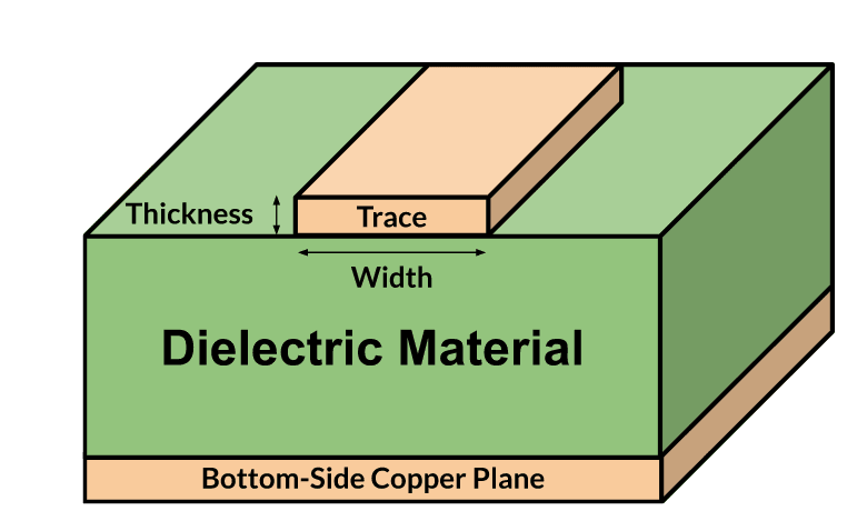
Understanding Copper Thickness Units: Mils and Ounces
Before diving into measurement techniques, let’s clarify the units used for copper thickness. In the PCB industry, copper is often measured in ounces per square foot (oz/ft2), which indicates the weight of copper over a specific area. This weight correlates to thickness: 1 oz/ft2 equals approximately 1.4 mils, 2 oz/ft2 equals about 2.8 mils, and so on. Some manufacturers also specify thickness directly in mils or micrometers (μm), where 1 mil is roughly 25.4 μm.
Knowing the target thickness for your design helps in selecting the right measurement method. For high-current applications, thicker copper (3 oz/ft2 or more) might be necessary, while standard signal boards often use 1 oz/ft2. Accurate measurement ensures compliance with these specifications.
Key Techniques for Measuring Copper Thickness on PCBs
There are several methods to measure copper thickness, each suited to different stages of the manufacturing process. These range from destructive techniques like microsectioning to non-destructive testing options that preserve the board. Below, we explore the most common approaches.
1. Microsectioning: A Destructive but Precise Method
Microsectioning is a widely used technique for measuring copper thickness with high accuracy. It involves cutting a small cross-section of the PCB, mounting it in resin, polishing it, and examining it under a microscope. This method allows for direct measurement of the copper layer thickness in mils or micrometers.
How It Works:
- A sample of the PCB is cut using a precision saw.
- The sample is embedded in a resin mold to hold it steady.
- It’s polished to expose a clear cross-section of the layers.
- Using a calibrated microscope, the copper thickness is measured at multiple points for consistency.
Advantages: Microsectioning provides precise results, often within ±0.1 mil accuracy, making it ideal for detailed quality control. It’s also useful for inspecting internal layers in multilayer boards.
Limitations: Since this is a destructive method, the tested sample cannot be reused. It’s typically performed on test coupons or scrap boards rather than final products.
2. Non-Destructive Testing: Preserving the PCB
For situations where destroying a sample isn’t an option, non-destructive testing (NDT) methods are invaluable. These techniques allow you to measure copper thickness without damaging the board, making them suitable for in-process checks during the manufacturing process.
Common NDT Methods:
- X-Ray Fluorescence (XRF): This method uses X-rays to excite the copper atoms, causing them to emit a detectable signal. The intensity of the signal correlates to the thickness of the copper layer. XRF is highly accurate, often within ±0.05 mils, and works well for both outer and inner layers.
- Eddy Current Testing: This technique measures changes in electrical conductivity caused by the copper layer. A probe generates an electromagnetic field, and the response is used to calculate thickness. It’s fast and effective for surface layers but less accurate for internal layers.
- Ultrasonic Testing: Using high-frequency sound waves, this method measures the time it takes for waves to reflect off the copper layer. It’s less common but useful for thicker copper deposits.
Advantages: NDT methods preserve the integrity of the PCB, allowing for 100% inspection if needed. They’re ideal for ongoing quality control in high-volume production.
Limitations: NDT equipment can be expensive, and accuracy may vary depending on the method and calibration. For instance, eddy current testing might struggle with very thin copper layers below 0.5 mils.
3. Beta Backscatter: A Specialized Non-Destructive Option
Beta backscatter is another non-destructive testing method that uses low-energy beta particles to measure copper thickness. The particles are emitted from a source and partially reflected by the copper layer. The amount of backscattered radiation is proportional to the thickness.
Advantages: This method is quick and works well for thin copper layers (0.1 to 2 mils). It’s often used in plating processes to monitor copper deposition.
Limitations: Beta backscatter requires specialized equipment and trained operators. It’s also less effective for thicker copper layers or complex multilayer boards.
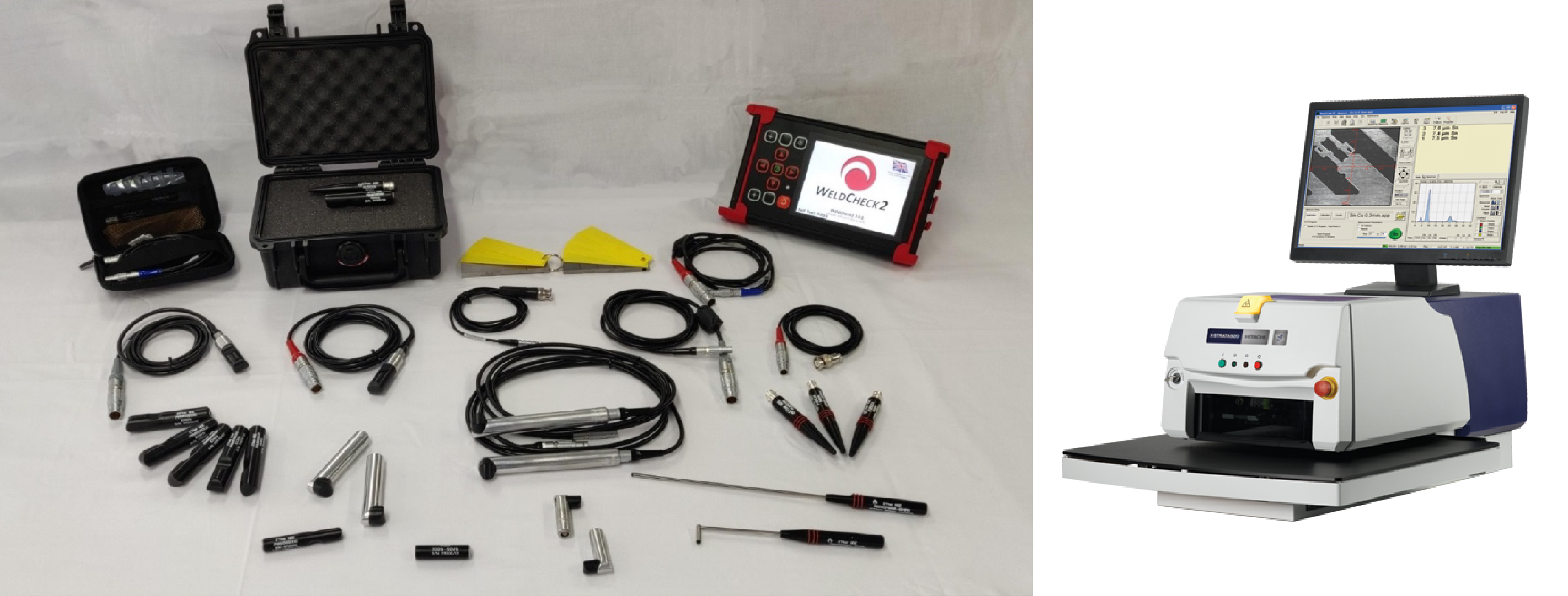
Tools for Measuring Copper Thickness on PCBs
Choosing the right tool depends on the measurement technique, budget, and production needs. Below are some commonly used tools for PCB copper thickness measurement.
1. Optical Microscopes for Microsectioning
For microsectioning, a high-quality optical microscope with digital imaging capabilities is essential. Look for models with magnification up to 1000x and software for precise measurements. These tools often cost between $2,000 and $10,000, depending on features.
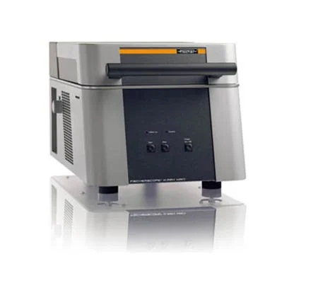
2. XRF Analyzers for Non-Destructive Testing
XRF analyzers are portable or benchtop devices used for non-destructive testing. They can measure copper thickness in seconds with high accuracy. Prices range from $10,000 to $50,000, making them a significant investment for quality control labs.
3. Eddy Current Probes
Eddy current probes are handheld or integrated into automated systems for quick surface measurements. They’re more affordable, with costs ranging from $1,000 to $5,000, and are ideal for spot-checking during the manufacturing process.
4. Beta Backscatter Gauges
These specialized tools are used in specific applications like plating thickness control. They’re less common and can cost upwards of $15,000, but they offer fast results for thin copper layers.
Best Practices for Accurate Copper Thickness Measurement
To ensure reliable results in PCB copper thickness measurement, follow these best practices during the manufacturing process:
- Calibrate Equipment Regularly: Whether using XRF analyzers or microscopes, calibration against known standards prevents errors. For example, calibrate XRF tools daily to maintain accuracy within ±0.05 mils.
- Measure Multiple Points: Copper thickness can vary across a board due to plating inconsistencies. Take measurements at several locations to get an average value.
- Use Test Coupons: For destructive methods like microsectioning, include test coupons in your PCB panel design. These are small sections made under the same conditions as the main board, allowing for testing without sacrificing the final product.
- Document Results: Keep detailed records of measurements for traceability in quality control. This helps identify trends or issues in the manufacturing process over time.
Challenges in Measuring Copper Thickness and How to Overcome Them
Despite the availability of advanced tools, measuring copper thickness can present challenges. Uneven plating, for instance, can result in thickness variations of up to 0.2 mils across a single board. To address this, use automated scanning tools like XRF to map thickness distribution.
Another issue is measuring internal layers in multilayer boards. While microsectioning is effective, it’s destructive. Non-destructive methods like XRF can sometimes penetrate to inner layers, but accuracy drops. In such cases, combining techniques or consulting with manufacturing experts can yield better results.
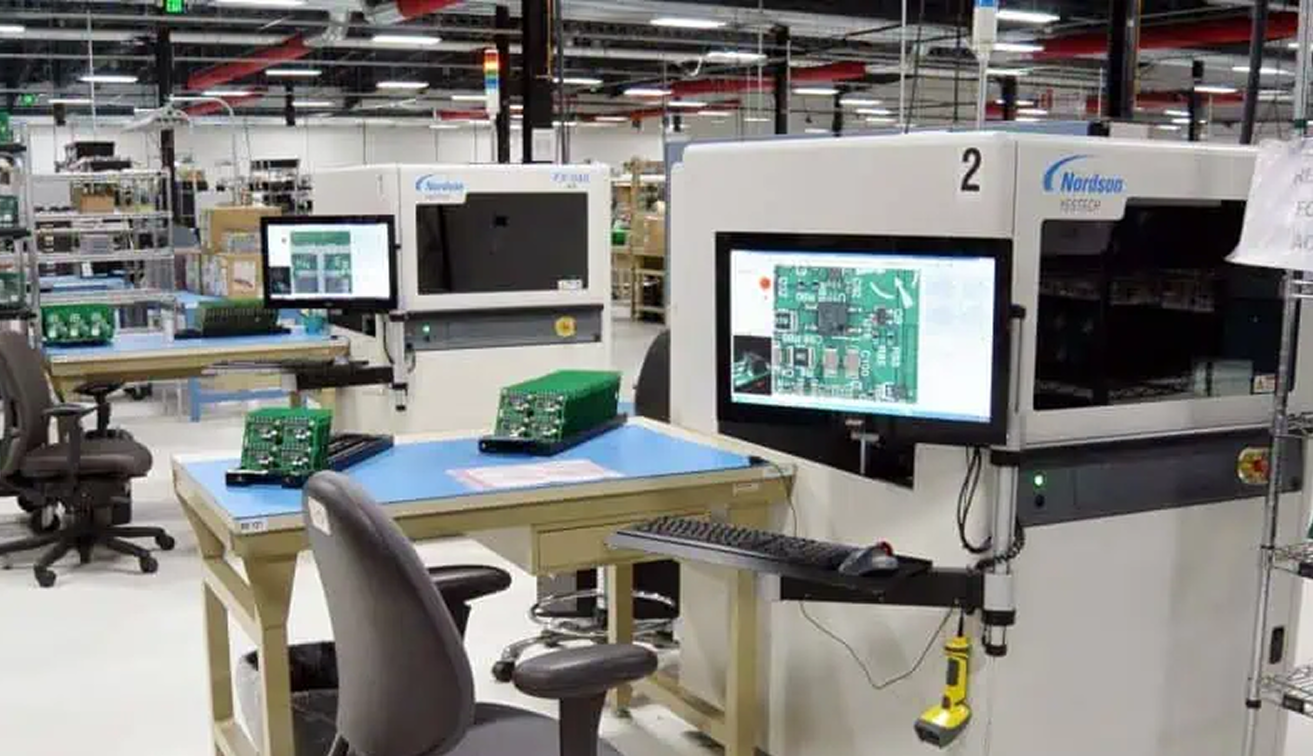
Integrating Measurement into Quality Control Processes
Copper thickness measurement isn’t just a one-time task; it should be part of a broader quality control strategy. During the manufacturing process, set specific checkpoints to measure thickness—after plating, before etching, and during final inspection. This ensures issues are caught early, reducing rework costs.
For high-volume production, consider automated non-destructive testing systems integrated into the production line. These can provide real-time data, allowing for immediate adjustments if thickness falls outside the target range (e.g., 1.4 mils ±0.1 mil for a 1 oz/ft2 layer).
Conclusion: Mastering Copper Thickness Measurement for Better PCBs
Accurate PCB copper thickness measurement is a cornerstone of reliable board design and production. Whether you opt for destructive methods like microsectioning or prefer non-destructive testing techniques such as XRF and eddy current testing, the right approach depends on your specific needs and resources. By using the tools and best practices outlined in this guide, you can ensure consistent quality control throughout the manufacturing process.
Investing in precise measurement not only prevents costly failures but also enhances the performance and lifespan of your PCBs. With a clear understanding of techniques and tools, you’re well-equipped to tackle copper thickness challenges and deliver top-notch results in every project.