 ALLPCB
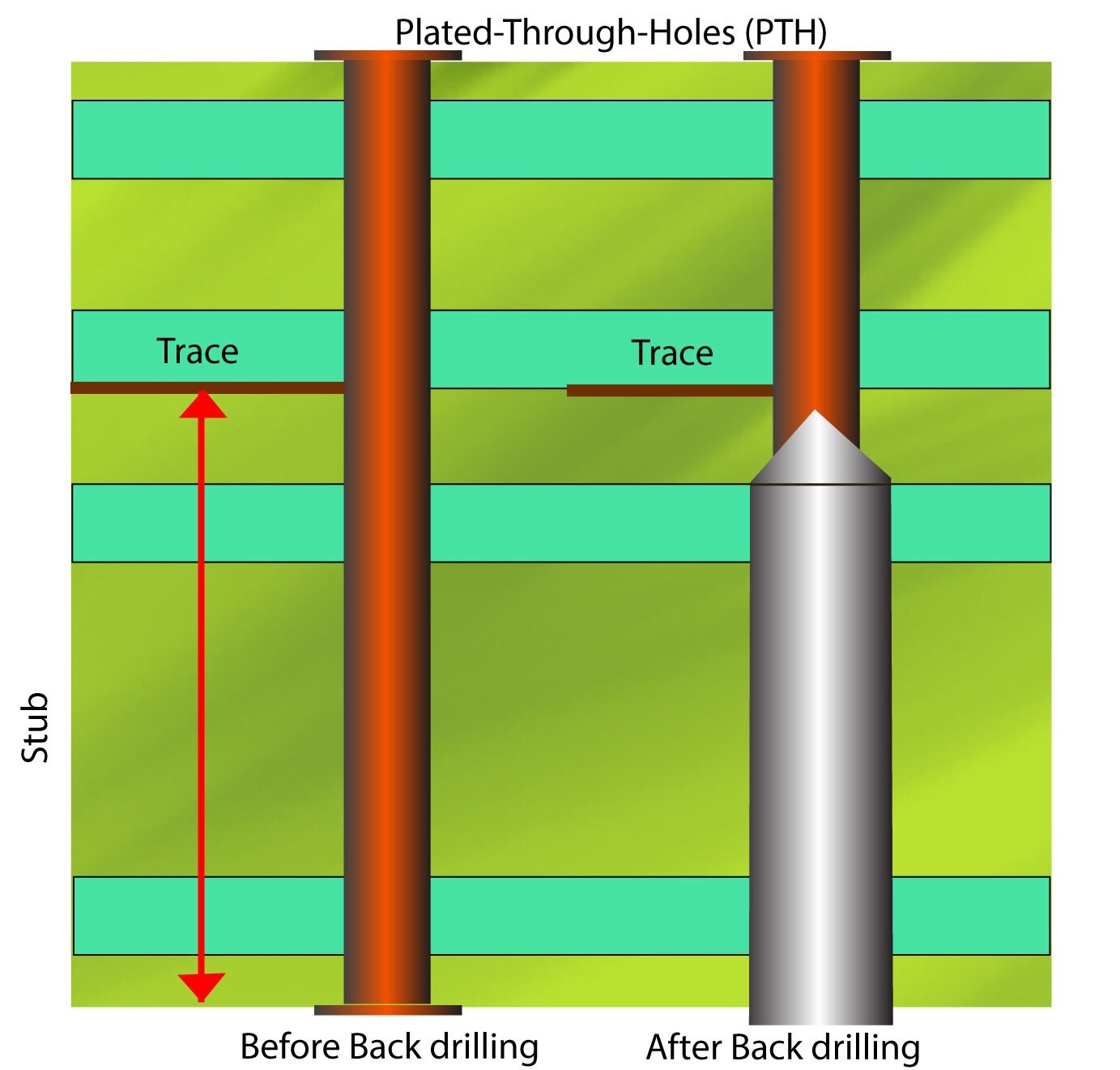
Backdrilling Design and Thermal Management: A Holistic Approach to PCB Design
Explore backdrilling and thermal management in PCB design for better signal integrity and heat dissipation with a holistic approach.


Explore backdrilling and thermal management in PCB design for better signal integrity and heat dissipation with a holistic approach.
Learn what a good PCB stack-up means for signal integrity, focusing on layers, impedance, return paths, and planes for optimal design.

Explore how trace spacing impacts impedance control, minimizes crosstalk, and reduces signal reflections in PCB design for optimal performance.
Optimize PCB layer stack-up for high-frequency designs to suppress crosstalk and minimize coupling with practical tips and stack-up examples.
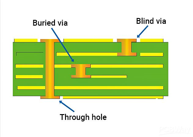
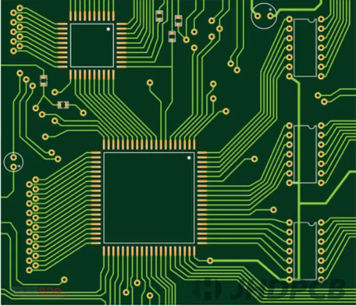
Learn about PCB vias, including through-hole, blind, and buried types, in this beginner tutorial on connecting layers with drilling and plating.

Master impedance control in PCB design with this guide on constraints, routing, matching, trace calculation, and differential impedance.

Explore PCB trace spacing, crosstalk, signal coupling, and manufacturing limits with practical tips on 3W rule, HDI, clearance, and DFM.

Learn BGA breakout design rules for manufacturability and reliability, focusing on clearances and spacing for optimal PCB performance.

Explore how copper pour affects PCB manufacturing costs, with strategies for cost reduction and optimal copper utilization in PCB design.
Explore backdrilling vs blind vias and buried vias in PCB design. Compare signal integrity, cost, and applications for optimal results.

Learn techniques for optimal BGA breakout signal integrity, focusing on impedance control and crosstalk reduction for high-speed PCB designs.

Beginner's guide to PCB design from schematic to Gerbers. Learn easy PCB design software, step-by-step tips, and online tutorials with ALLPCB.

Explore advanced PCB routing techniques using constraint management for high-speed, differential pair, and controlled impedance designs with ALLPCB.

Explore copper pour balancing in PCB design for reliability, warping prevention, signal integrity, and thermal management benefits.
ALLPCB delivers optimized PCB copper pour solutions. From plating balance to thermal stability, our copper pouring expertise ensures reliable, high-performance boards.
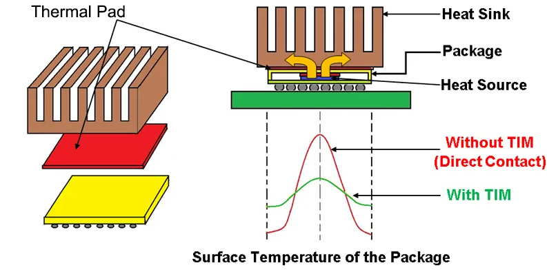
Learn how to choose the ideal thermal pad thickness for your application with tips on compression, gap fillers, and stress analysis at ALLPCB.
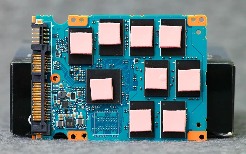
Learn how to use thermal pads for heat dissipation with this beginner's guide. Discover application tips, thickness choices, and easy thermal management.

Learn hobbyists! Discover easy-to-use PCB schematic tools and free design software for beginners to kickstart your electronics journey.
Learn PCB trace width calculation with this step-by-step guide for hobbyists. Master current, temperature, and IPC-2221 tips easily!
Explore best practices for SMT design, covering component placement, stencil design, reflow optimization, equipment, and defect troubleshooting.